
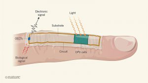
Motivation
Traditional silicon electronics have allowed us to follow the trend predicted by Moore’s Law, doubling process power roughly every two years. If we are to continue this trend, we need alternative electronics. Additionally, non-traditional semiconductors can provide other desirable properties like printability and flexibility, lower cost, and lower weight. Potential applications include printed large-area solar cells, flexible displays, and wearable “lab-on-skin” sensors that power themselves with solar energy (See Figure 1). Recent research into 2D atomic layered materials like graphene and MoS2 usher in a whole new set of possibilities.
Generally, the electrical performance of these materials depends strongly on the number and location of defects within the deposited layers, interfaces and the local environment, and changes induced by biasing them with an electric field over an extended time. It is vital to be able to investigate defects on the scale of the defects themselves. Typical measurements instead average over an area that includes many defects and possibly multiple interfaces. Our lab specializes in challenging and creative uses of atomic force microscopy (AFM), along with standard electrical transport measurements. Kelvin Probe Force Microscopy (KPFM) is a mode of operation of the AFM allowing direct measurement of surface potentials with spatial resolution of a few tens of nanometers, correlated with high resolution topographic images. Under the right conditions, KPFM can be used to measure the density of states in a material. We are developing a technique to study the real-time motion of charges in thin films, which can measure the filling and emptying of trap states, which is particularly important to understand in materials where traps dominate the transport.
Types of Materials Studied in the Lab
Organic semiconductors
Organic semiconductors are particularly exciting for their applications with low cost, flexible electronics. Imagine rolling up your “computer” into the width of a pencil, covering parking lots with awnings filled with solar cells, or having a display on the contact lens in your eye. Commercial OLED displays use these materials, and the recently released foldable phones make use of their flexibility. While the optical properties of these materials hold tremendous promise with low cost fabrication techniques, the electrical properties are often dominated by traps, interfaces, and can be unstable over time. We work in collaboration with the Arango Lab at Mount Holyoke to explore a range of materials relevant to the photovoltaics fabricated in their lab. These materials include P3HT, full name poly(3-hexylthiophene-2,5-diyl), a frequently studied hole majority carrier organic semiconductor, and PDI-CN2, a perylene diimide, which is an electron majority carrier. Check out Xinrui (Anna) Zhu’s APS March Meeting 2020 talk on evidence for an accumulation layer at the donor-acceptor interface in organic solar cells here.
Nanocrystal Quantum Dots

Nanocrystal (aka “colloidal”) Quantum Dots (QDs) are roughly spherical nanoscale chunks of crystalline material with a diameter of generally less than 10nm. When materials are restricted to this size range, their electronic properties change dramatically due to quantum confinement. A quantum dot is the real-life implementation of the “particle in a box” that undergraduates solve in their quantum mechanics class. The quantum confinement leads to quantized energy levels. The narrower the diameter, the larger the energy level spacing. This results in different wavelength emission of light (redder for larger QDs, bluer for smaller QDs), such that by changing only the diameter of the QD, one can control the wavelength of light. QLED televisions are a commercial application of this technology, along with fluorescent labels for microscopy. Our collaborators in the Arango Lab study PbS QDs in solar cells.
Perhaps unsurprisingly, the electronic properties of QDs are highly dependent on their immediate environment. A single trapped charge can impact the electrical and optical properties. Presently, the optical properties of QDs are better studied than the electronic properties of arrays of the QDs. We are presently focusing on the electrical properties of PbS quantum dots.
2D Atomic Layered Materials
Materials like graphene form strong bonds in two-dimensions, while weakly interacting between layers through van der Waals forces (e.g. graphite). Since the discovery in 2004 that single layers of graphene could be controlled in the research lab, many researchers have been studying the unique properties of this class of materials that arise due to the quantum mechanical confinement to two dimensions. Our lab is presently interested in the properties of semiconductor MoS2, in collaboration with Jing Kong’s lab at MIT, as part of the NSF funded Center for Integrated Quantum Materials. Check out Christina McGahan’s APS March Meeting 2020 talk on comparative electrical scanning probe measurements on doped monolayer MoS2 here.