
Kelvin Probe Force Microscopy records the electrical potential at the surface of the sample. One way to think about how it works is to consider the tip and the sample as a capacitor. If there is a potential difference between the sample and tip, there will be an electric field, and the tip will experience a force. We actually oscillate the tip by applying a small ac electrical signal at the resonance frequency, leading to an amplitude of oscillation. A DC feedback loop then alters the DC voltage of the tip until the applied voltage is equal to the potential at the surface of the sample, minimizing the force the tip feels and minimizing the amplitude of oscillation. By plotting the applied DC voltage at each point that minimizes the oscillation, we record the potential of the device. Most commonly, researchers use this technique to measure the workfunction of different materials with nanoscale resolution. Any contributions to the electric potential at the surface will contribute to the recorded voltage of the feedback loop, which includes trapped charges and intentionally applied voltages. Figure 1 shows a typical topography and potential image of a device that has two gold electrodes on either side and a channel of the organic semiconductor P3HT between them. The left electrode is grounded, and the right electrode is near 3 V. Use the slider to shift between the topography and potential image.
We have developed a technique that measures the real-time injection and extraction of charges on the scale of milliseconds, a relevant time-scale for many disordered non-traditional semiconductors with transport that can be dominated by traps. By using an FET geometry with a backgate (see Figure 2), and grounding the source and drain electrodes, we can record the real-time screening of the potential applied to the gate. We step the gate voltage, which results in an immediate change in the potential measured by the tip. Over time, charges rush in or out of the film, screening this potential, as illustrated in Figure 2.
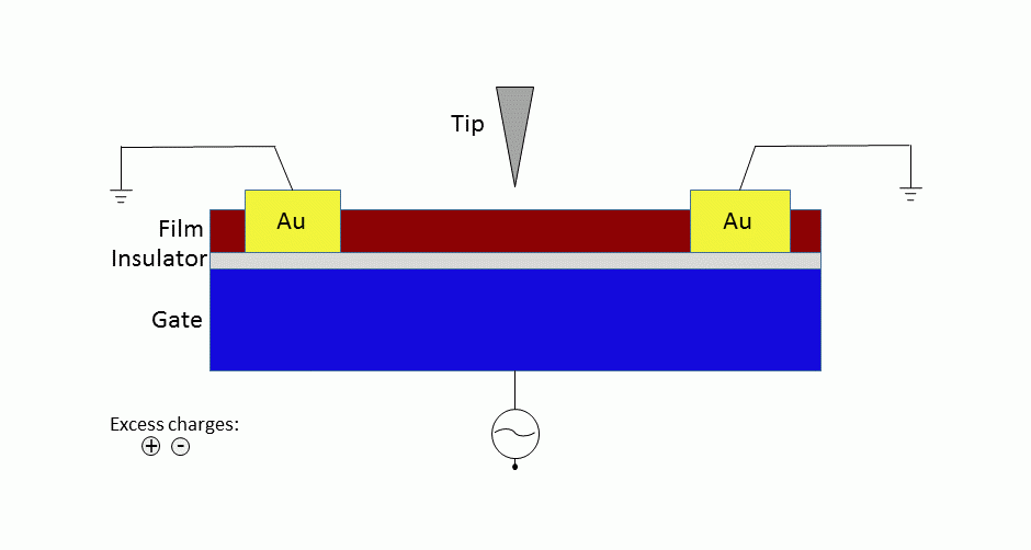
Figure 2: Cartoon of the time resolved KPFM setup. An FET with a backgate allows us to position the tip above the materials that we are studying. By stepping the gate voltage (negative in this case), charges (positive) rush into the film from the grounded electrodes in response to the electric field, eventually screening the field from the tip.
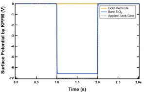
Figure 3 shows a control sample, without a semiconducting film. The dotted black line is the voltage applied to the gate, -7V in this case. The yellow line is the potential the tip records above the grounded gold electrode. Unsurprisingly, the line is constant at zero, because the electrons in the gold move so quickly in response to the gate voltage that we do not see any change in potential. When the tip is instead placed over the silicon dioxide insulator, the blue line results. The tip records a negative step in potential, following gate voltage. We fit an exponential to the rise time and find a time constant of 3ms, giving us our time resolution for this experiment.
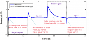
Figure 4 shows data from a P3HT film. As the gate voltage is stepped negative, the tip records a momentary negative potential, which returns to zero as the holes are injected into the film from the gold electrodes, screening the potential. As the gate voltage is stepped back to zero, there is an initial surplus of holes in the film, resulting in a momentary positive potential, which returns to zero as holes exit the film. For the positive gate voltage, there is an initial positive potential recorded by the tip that returns to zero as more holes leave the film. Returning the gate voltage to zero results in a momentary negative potential recorded by the tip as there are initially too few holes in the film. In response to the gate voltage change, holes are injected and the potential returns to zero. We can see by eye that it takes longer to extract holes than inject holes. This can be understood by considering the role that traps play in transport in this sample. As carriers enter the film, some fall into traps. This can happen quickly, so injecting the holes happens quickly. When the holes must be extracted, some are caught in these traps, and so it takes longer for the holes to exit the film. For more information, see Moscatello et al., Organic Electronics, 41, 26 (2017), which compares the results on an electron majority carrier and examines the effect of bias stress.